3F,Block C,No.179 Guangpu East Road, Huangpu District, Guangzhou, GD, China


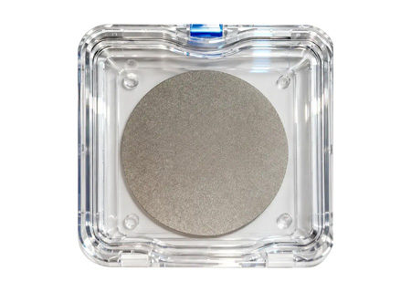
Deposon polycrystalline diamond is produced by MPCVD equipment using a hetero-nucleation process. The grains are dense with a seamless continuous phase, and thermal conductivity covers multiple grades from 1000–1800 W/(m·K). With lower cost and shorter lead times, it provides large-area diamond materials for heat spreaders, thermal substrates, and optical windows.
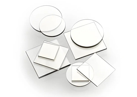
Homoepitaxially grown by MPCVD on high-quality single-crystal seed crystals, with controllable crystal defects and stable batch-to-batch consistency. Delivered in application-specific grades, with customization supported.
High-thermal-conductivity heat spreaders and thermal substrates
High-power laser windows and Raman optical devices
Boron-doped conductive diamond
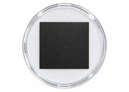
Deposon diamond flexible films are made by releasing a CVD diamond layer from its growth substrate, forming a fully free-standing, independent diamond film — with no dependence on adhesive tape, polymers, or rigid carriers, and therefore none of the additional thermal resistance or outgassing associated with adhesive layers.
While retaining diamond's intrinsic high thermal conductivity and electrical insulation, the film gains macroscopic bendability, can conform to curved surfaces and irregularly shaped heat sources, supports laser cutting and drilling, and can be delivered in any planar shape.
800–1500 W/(m·K)
5–30 μm
Customized on demand, max diameter 300 mm
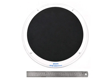
Deposon silicon-based diamond grows a continuous-phase CVD diamond layer directly on silicon wafer substrates via a hetero-nucleation process — with no adhesive layer and no seams between diamond and silicon, and interface thermal resistance approaching zero.
The silicon substrate retains physical properties fully compatible with mainstream semiconductor processes: its coefficient of thermal expansion matches Si/GaN/SiC devices, and it can directly undergo eutectic bonding, direct bonding, and flip-chip interconnects. The diamond layer laterally spreads hotspot heat at 1000–1800 W/(m·K). Size and thickness are customized on demand, adapting to 2.5D/3D packaging and Chiplet architectures, mitigating thermal coupling between stacked chips, and shortening the heat dissipation path of advanced packaging by an order of magnitude.
2 / 3 / 4 / 6 / 8 / 12 inches
750 μm – 8 mm
100 nm – 500 μm
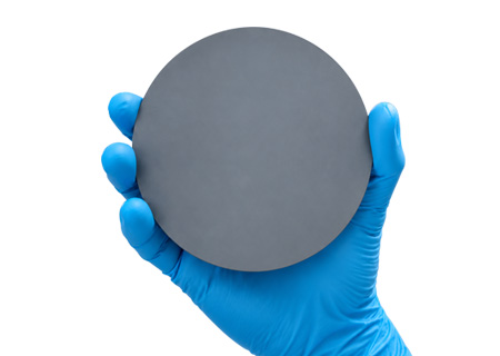
Deposon ceramic-based diamond grows a continuous-phase CVD diamond layer directly on non-oxide ceramic substrates such as silicon carbide (SiC), silicon nitride (Si₃N₄), and aluminum nitride (AlN) via a hetero-nucleation process — with no adhesive layer and no seams between diamond and ceramic, and interface thermal resistance approaching zero.
The ceramic substrate is itself the standard insulating base for power packaging: electrically insulating with high breakdown voltage, and a coefficient of thermal expansion matched to SiC/GaN chips. The diamond layer laterally spreads hotspot heat at 1000–1800 W/(m·K). Substrate material, size, and thickness are customized on demand; the product is compatible with bonding and metallization processes, and adapts to GaN/SiC power modules, RF power amplifiers, and high-power lasers — driving device junction temperatures down another notch without sacrificing insulation performance.
SiC / Si₃N₄ / AlN (other materials can be evaluated)
Customized on demand; full panels and small-piece dicing supported
0.25 – 1.5 mm
100 nm – 500 μm
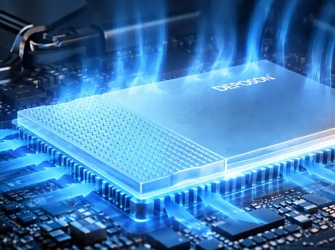
The hotspot heat flux of GPUs, CPUs, and Chiplet advanced packaging has exceeded the capacity of conventional thermal materials. Deposon silicon-based diamond can be directly bonded to chips, building high-efficiency heat conduction channels at the positions closest to the heat source.
Power semiconductors face equally severe challenges — the local heat flux of GaN and SiC devices can reach 5 to 10 times the average. Ceramic-based diamond and diamond heat spreaders attach directly to the chip heat source, significantly reducing junction temperature and leaving greater headroom for power density and device lifetime.
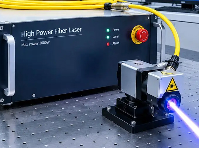
In the laser industry, diamond heat spreaders have become the mainstream thermal substrate for high-power semiconductor laser bars and fiber laser pump sources. RF communication devices such as GaN power amplifiers for 5G base stations and radar T/R modules have also achieved higher output power and long-term reliability through diamond cooling solutions.
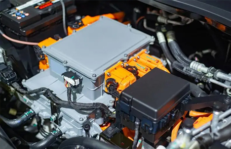
The adoption of 800 V platforms in new energy vehicles is driving the power density of SiC main-drive inverters and on-board chargers ever higher, and diamond thermal substrates are opening a next-generation thermal management path for automotive-grade power modules.

In optical communications, the laser chips in 800G / 1.6T high-speed optical modules impose stringent temperature-control precision requirements. Diamond heat spreaders effectively suppress wavelength drift and safeguard link stability.

As per-rack power in data centers moves toward 100 kW, the cooling of server power supplies and power modules is also beginning to rely on the support of diamond materials.

Diamond combines radiation resistance with ultra-high thermal conductivity, making it an ideal choice for lightweight thermal control of satellite-borne power amplifiers and phased-array antennas. Diamond flexible films can conform to curved surfaces and irregular devices, offering a completely new option for flexible electronics cooling that conventional rigid materials cannot achieve.